Image Sensor and Solar Cell
Image Sensor
Application Example for Download

CMOS image sensor simulation, including process:
- reset
- illumination
- readout
Example
Structure
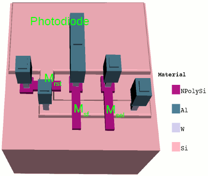
The example three-dimensional CMOS image sensor cell structure is generated by Gds2Mesh tool. Ray-Tracing method is used for light propagation simulation, and TCAD simulation is implemented by Genius. These physical varieties can be analyzed or optimized quantitatively though our simulation:
- Internal quantum efficiency
- Dark current
- Dynamic range
In the example, the CMOS image sensor consists of three transistors (3T) and a photo-diode. The photo-diode, Dphoto, consists of an N+ impurity layer in a P-well. The three transistors are the photo-diode reset transistor, Mrst, the amplifier transistor Msf, and the select transistor Msel, as shown in figure above.
Illumination Integration

Figure above gives the simulated voltage of the photo-diode Vpd under the different illumination intensities (dark condition, 0.01W/cm2, and 0.1W/cm2). The incident wavelength is 0.55um. The decrease in the voltage Vpd is approximately proportional to illumination intensity. And the CMOS image sensor reaches saturation at the illumination intensity 0.1W/cm2.
Readout
Figure below gives the simulated readout voltage from node Vout, compared with the voltage from node Vpd.

Solar Cell
Three factors are responsible for light intensity losses in solar cells:
- The Si surface reflects 35%-50%, depending upon incident wavelength.
- The grid structure shadows 3%-12%, depending upon the designing of the grid.
- Absorption in silicon (indirect semiconductor) is very low in the long wavelength sunlight range, i.e., near to the band edge. And light absorbed in the back surface contact produces none photo-voltaic effect.
Various technological methods are implemented to prevent or reduce these losses.
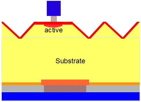
An anti-reflection effect can be achieved in two different ways. One is by a thin film of ‘anti-reflection coating’, and the other is by texturizing of the cell surface. As shown in figure below, the surface is structured so that multiple reflections allow most of the light to be absorbed in the cell.


The physical models would be considered in simulation:
- Ray-tracing optics
- Anti-reflective coating
- Doping dependent carrier lifetime
- Surface recombination
The simulated IV curve of the cell is shown in figure below.


